Elisa Riedo
-
Herman F. Mark Professor in Chemical and Biomolecular Engineering
-
Professor of Physics at NYU’s College of Arts and Science
-
Director, Faculty Development

Elisa Riedo is Professor of Chemical and Biomolecular Engineering at New York University Tandon School of Engineering. She is also Professor of Physics at NYU College of Arts and Science and affiliated Professor of Mechanical Engineering. Previously, Riedo was Professor of Physics at the Georgia Institute of Technology from 2003 to 2015. She graduated summa cum laude in Physics at the University of Milano, and obtained a Ph.D. in Physics in 2000 with a joint thesis between the University of Milano, and the European Synchrotron Research Facility (ESRF) in Grenoble, France. She then worked as postdoctoral fellow at the Ecole Polytechnic Federale de Lausanne (EPFL) in Switzerland. She is particularly well known for her pioneering work in thermal scanning probe lithography (tSPL), a novel and sustainable nanofabrication technique with applications in biomedicine, nanoelectronics, and magnetic materials. She has also made fundamental contributions in nanomechanics, graphene, diamene, 2D materials, and nano-confined water. She is widely published, and has received multiple grants from the National Science Foundation, the Department of Energy, and the Department of Defense. She is a Fellow of the American Physical Society.
Education
University of Milano, Italy 2000
Ph.D., Physics
University of Milano, Italy 1995
B.S., Physics
Information for Mentees
Mentoring Style: Informal, open discussions, sense of humor, like mixing work and good food
My Science: Nanoelectronics, NanoBioTechnology, Nanomechanics
Publications
Selected Publications:
“Cost and Time Effective Lithography of Reusable Millimeter Size Bone Tissue Replicas With Sub‐15 nm Feature Size on A Biocompatible Polymer”, Advanced Functional Materials (2021) https://doi.org/10.1002/adfm.202008662. (Cover Article)
“Pressure-induced formation and mechanical properties of 2D diamond boron nitride”, Advanced Science (2021) 8, 2002541, https://doi.org/10.1002/advs.202002541. (Cover Article)
“Nanofabrication of graphene field-effect transistors by thermal scanning probe lithography”, Applied Physics Letters Materials (2021) 9 (1), 011107 https://doi.org/10.1063/5.0026159
“Spatial Defects Nanoengineering for Bipolar Conductivity in MoS2”, Nature Communications (2020) https://www.nature.com/articles/s41467-020-17241-1
”Patterning metal contacts on monolayer MoS2 with vanishing Schottky barrier using thermal nanolithography”, Nature Electronics 17–25 (2019) https://doi.org/10.1038/s41928-018-0191-0
“Ultra-hard carbon film from epitaxial two-layer graphene” Nature Nanotechnology 13, (2018), doi:10.1038/s41565-017-0023-9
“Nanopatterning reconfigurable magnetic landscapes via thermally assisted scanning probe lithography” Nature Nanotechnology, 11, 545–551 (2016) (Cover article)
“Elastic coupling between layers in two-dimensional materials”, Nature Materials 14, 714–721 (2015)
“Advanced Scanning Probe Lithography”, Nature Nanotechnology, 9, 577 (2014).
“Room Temperature Metastability of Multilayer Epitaxial Graphene Oxide”, Nature Materials, 11, 544, (2012).
"Nanoscale Tunable Reduction of Graphene Oxide for Graphene Electronics," Science, 328, 1373-1376, (2010).
“Structured and viscous water in subnanometer gaps”, Phys. Rev. B 75, 115415 (2007).
“Elastic Property of Vertically Aligned Nanowires/Nanotubes”, Nano Letters 12, 1954 (2005).
“Radial Elasticity of Multiwalled Carbon Nanotubes”, Phys. Rev. Lett. 94, 175502, (2005).
Research News

Study Shows New Method to Produce Ultrahard Single Layer Diamond in Industrial Applications
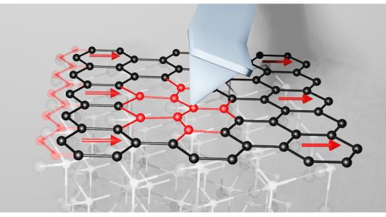
Graphene’s enduring appeal lies in its remarkable combination of lightness, flexibility, and strength. Now, researchers have shown that under pressure, it can briefly take on the traits of one of its more glamorous carbon cousins. By introducing nitrogen atoms and applying pressure, a team of scientists has coaxed bilayer graphene grown through chemical vapor deposition (CVD) into a diamond-like phase — without the need for extreme heat. The finding, reported in Advanced Materials Technologies, shows a scalable way to create ultrathin coatings that combine the toughness of diamond with the processability of graphene.
The work, led by Elisa Riedo, Herman F. Mark Professor in Chemical and Biomolecular Engineering, focuses on the delicate balance between two forms of carbon bonding. In ordinary graphene, carbon atoms connect through sp² bonds in a flat honeycomb arrangement, giving rise to its electrical conductivity and mechanical toughness. Diamond, on the other hand, is built from sp³ bonds in a three-dimensional network that confers exceptional hardness. Converting one to the other typically demands extreme pressure and temperature. The team discovered that nitrogen doping lowers this barrier, allowing the transition to occur at room temperature when the layers are pressed together.
To test the effect, the researchers used CVD bilayer graphene films on silicon dioxide substrates and incorporated nitrogen atoms during the growth process. They then applied mechanical pressure using a technique known as modulated nanoindentation. The nitrogen-doped bilayer films exhibited nearly twice the stiffness of the bare substrate, suggesting the formation of stronger, diamond-like interlayer bonds. By contrast, nitrogen-doped monolayer or thicker multilayer samples showed no comparable stiffening, indicating that the effect depends on both the doping and the precise bilayer structure.
Molecular dynamics simulations provided a possible explanation. The models showed that nitrogen atoms promote the formation of sp³ bonds between the two layers when they are compressed. The nitrogen atoms appear to stabilize these interlayer bonds, effectively “locking” parts of the bilayer into a more diamond-like configuration. This cooperation between chemical doping and pressure points to a previously unrecognized pathway for transforming graphene’s atomic structure.
The implications extend beyond a mere curiosity of carbon chemistry. Because the experiments used large-area graphene grown by chemical vapor deposition, the process is inherently compatible with industrial fabrication methods and wafer scale dimensions. The transformation also occurs under mild conditions, avoiding the high temperatures that typically destroy or distort 2D materials. In principle, the approach could yield ultrathin, lightweight coatings that resist wear and deformation while maintaining the advantages of graphene substrates.
Yet the work raises as many questions as it answers. The extent of the transformation remains uncertain — whether the sp³ bonding is continuous or confined to localized regions under the indenter is not yet clear. Researchers also do not know whether the diamond-like phase persists once the pressure is released, or whether it relaxes back to graphene over time. Understanding how stable and uniform these transformations are will be critical for any practical use.
The effect on electronic behavior also remains to be seen. Diamond-like carbon is typically an electrical insulator, so localized sp³ regions could alter the electronic or optical properties of the film. For device applications, the challenge will be to tune the process so that mechanical and electrical properties can be balanced rather than compromised.
Future research will need to clarify how doping levels, pressure intensity, and substrate choice influence the transformation.
The study suggests that graphene’s versatility may stretch further than expected. By manipulating its atomic environment — through doping, strain, or pressure — researchers may be able to switch between distinct structural phases on demand. Such control could lead to a new generation of adaptive materials, capable of shifting from soft to hard, or from conductive to insulating, depending on their operating conditions.
Graphene has often been described as a material with untapped potential. This work offers another glimpse of that potential, showing that even after more than a decade of intense study, carbon’s simplest form still has surprises left to offer.
This work was supported by the U.S. Army Research Office.

NYU Tandon engineers develop new transparent electrode for infrared cameras
Infrared imaging helps us see things the human eye cannot. The technology — which can make visible body heat, gas leaks or water content, even through smoke or darkness — is used in military surveillance, search and rescue missions, healthcare applications and even in autonomous vehicles.
These capabilities come with an engineering challenge, however. Infrared cameras need electrical contacts to capture and transmit the images they detect. Most materials that can conduct electrical signals also block the majority of infrared radiation from reaching the sensor, creating a fundamental conflict between seeing infrared light and having the electrical connections needed to process that information.
To solve this, researchers at NYU Tandon School of Engineering have developed a transparent electrode made from embedding tiny silver wires, similar in width to human hair, into a transparent plastic matrix that can be simply deposited on top of conventional infrared detectors.
The research, published in the Journal of Materials Chemistry C and recently selected as a HOT article by the journal's editors, tackles a key challenge in infrared detector manufacturing.
"We've developed a material that solves a fundamental problem that has been limiting infrared detector design," said Ayaskanta Sahu, associate professor in the Department of Chemical and Biomolecular Engineering (CBE) at NYU Tandon and the study's senior author. "Our transparent electrode material works well across the infrared spectrum, giving engineers more flexibility in how they build these devices."
The researchers tested their material by building it into infrared cameras that use colloidal quantum dots as the light-responsive material. These are tiny engineered particles that have recently gained attention for their use in quantum dot televisions and their role in earning the 2023 Nobel Prize in Chemistry. For this study, the group specifically used tiny clusters of mercury telluride, a type of quantum dot that responds to various wavelengths of infrared light.
Their new approach represents a significant improvement over existing methods. Traditional infrared photodetectors have relied on expensive materials like indium tin oxide (ITO) or thin metal films, which either lose transparency in longer infrared wavelengths or suffer from poor electrical properties and must be rigid.
Measuring 120 nanometers in diameter and 10-30 micrometers in length, the silver nanowires form conductive networks even at relatively low concentrations. When embedded in the PVA matrix, they form a silvery conductive ink that can be sprayed or spun onto infrared detectors as stable and flexible films that can even be manufactured at the low temperatures needed for quantum dot processing.
"Conventional electrodes in the infrared are like blackout curtains — most of the signal never reaches the sensor," said graduate researcher Shlok J. Paul, a co-author on the study. "Our near-invisible web of silver nanowires lets more infrared photons in while doubling as the wiring that carries the electrical current needed to turn the invisible light into data. While there is more work to be done, the simplicity of this flexible layer could carry IR detection from the lab to commercial applications like for firefighter vision or self-driving cars.”
In addition to Sahu and Paul, the paper's authors are Elisa Riedo, Herman F. Mark Professor in NYU Tandon's CBE Department, and graduate students Håvard Mølnås, Steven L. Farrell, and Nitika Parashar, all from CBE as well.
The work was supported by the Defense Advanced Research Projects Agency, the Office of Naval Research, the US Army Research Office, and the National Science Foundation.
The researchers filed a U.S. patent application covering their method for embedding silver nanowires in a polymer matrix for transparent infrared electrodes.
Paul, Shlok J., et al. “Plenty of room at the top: Exploiting nanowire – polymer synergies in transparent electrodes for infrared imagers.” Journal of Materials Chemistry C, vol. 13, no. 21, 2025, pp. 10592–10601

Out of thin air: Researchers create microchips capable of detecting and diagnosing diseases
In a world grappling with a multitude of health threats — ranging from fast-spreading viruses to chronic diseases and drug-resistant bacteria — the need for quick, reliable, and easy-to-use home diagnostic tests has never been greater. Imagine a future where these tests can be done anywhere, by anyone, using a device as small and portable as your smartwatch. To do that, you need microchips capable of detecting miniscule concentrations of viruses or bacteria in the air.
Now, new research from NYU Tandon faculty including Professor of Electrical and Computer Engineering Davood Shahrjerdi; Herman F. Mark Professor in Chemical and Biomolecular Engineering Elisa Riedo; and Giuseppe de Peppo, Industry Associate Professor in Chemical and Biomolecular Engineering and who was previously at Mirimus, shows it’s possible to develop and build microchips that can not only identify multiple diseases from a single cough or air sample, but can also be produced at scale.
“This study opens new horizons in the field of biosensing. Microchips, the backbone of smartphones, computers, and other smart devices, have transformed the way people communicate, entertain, and work. Similarly, today, our technology will allow microchips to revolutionize healthcare, from medical diagnostics, to environmental health” says Riedo,
“The innovative technology demonstrated in this article uses field-effect transistors (FETs) — miniature electronic sensors that directly detect biological markers and convert them into digital signals — offering an alternative to traditional color-based chemical diagnostic tests like home pregnancy tests,” said Shahrjerdi. “This advanced approach enables faster results, testing for multiple diseases simultaneously, and immediate data transmission to healthcare providers” says Sharjerdi, who is also the Director of the NYU Nanofabrication Cleanroom, a state-of-the-art facility where some of the chips used in this study were fabricated. Riedo and Shahrjerdi are also the co-directors of the NYU NanoBioX initiative.
Field-effect transistors, a staple of modern electronics, are emerging as powerful tools in this quest for diagnostic instruments. These tiny devices can be adapted to function as biosensors, detecting specific pathogens or biomarkers in real time, without the need for chemical labels or lengthy lab procedures. By converting biological interactions into measurable electrical signals, FET-based biosensors offer a rapid and versatile platform for diagnostics.
Recent advancements have pushed the detection capabilities of FET biosensors to incredibly small levels — down to femtomolar concentrations, or one quadrillionth of a mole — by incorporating nanoscale materials such as nanowires, indium oxide, and graphene. Yet, despite their potential, FET-based sensors still face a significant challenge: they struggle to detect multiple pathogens or biomarkers simultaneously on the same chip. Current methods for customizing these sensors, such as drop-casting bioreceptors like antibodies onto the FET’s surface, lack the precision and scalability required for more complex diagnostic tasks.
To address this, these researchers are exploring new ways to modify FET surfaces, allowing each transistor on a chip to be tailored to detect a different biomarker. This would enable parallel detection of multiple pathogens.
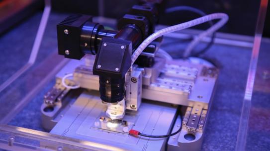
Enter thermal scanning probe lithography (tSPL), a breakthrough technology that may hold the key to overcoming these barriers. This technique allows for the precise chemical patterning of a polymer-coated chip, enabling the functionalization of individual FETs with different bioreceptors, such as antibodies or aptamers, at resolutions as fine as 20 nanometers. This is on par with the tiny size of transistors in today’s advanced semiconductor chips. By allowing for highly selective modification of each transistor, this method opens the door to the development of FET-based sensors that can detect a wide variety of pathogens on a single chip, with unparalleled sensitivity.
Riedo, who was instrumental in the development and proliferation of tSPL technology, sees its use here to be further evidence of the groundbreaking way this nanofabrication technique can be used in practical applications. “tSPL, now a commercially available lithographic technology, has been key to functionalize each FET with different bio-receptors in order to achieve multiplexing,” she says.
In tests, FET sensors functionalized using tSPL have shown remarkable performance, detecting as few as 3 attomolar (aM) concentrations of SARS-CoV-2 spike proteins and as little as 10 live virus particles per milliliter, while effectively distinguishing between different types of viruses, including influenza A. The ability to reliably detect such minute quantities of pathogens with high specificity is a critical step toward creating portable diagnostic devices that could one day be used in a variety of settings, from hospitals to homes.
The study, now published by the Royal Society of Chemistry in Nanoscale, was supported by Mirimus, a Brooklyn-based biotechnology company, and LendLease, a multinational construction and real estate company based in Australia. They are working with the NYU Tandon team to develop illness-detecting wearables and home devices, respectively.
“This research shows off the power of the collaboration between industry and academia, and how it can change the face of modern medicine,” says Prem Premsrirut, President and CEO of Mirimus. “NYU Tandon’s researchers are producing work that will play a large role in the future of disease detection.”
“Companies such as Lendlease and other developers involved in urban regeneration are searching for innovative solutions like this to sense biological threats in buildings.” says Alberto Sangiovanni Vincentelli of UC Berkeley, a collaborator on the Project. “Biodefense measures like this will be a new infrastructural layer for the buildings of the future”
As semiconductor manufacturing continues to advance, integrating billions of nanoscale FETs onto microchips, the potential for using these chips in biosensing applications is becoming increasingly feasible. A universal, scalable method for functionalizing FET surfaces at nanoscale precision would enable the creation of sophisticated diagnostic tools, capable of detecting multiple diseases in real time, with the kind of speed and accuracy that could transform modern medicine.

Discovery of new growth-directed graphene stacking domains may precede new era for quantum applications
Graphene, a single layer of carbon atoms arranged in a two-dimensional honeycomb lattice, is known for its exceptional properties: incredible strength (about 200 times stronger than steel), light weight, flexibility, and excellent conduction of electricity and heat. These properties have made graphene increasingly important in applications across various fields, including electronics, energy storage, medical technology, and, most recently, quantum computing.
Graphene’s quantum properties, such as superconductivity and other unique quantum behaviors, are known to arise when graphene atomic layers are stacked and twisted with precision to produce “ABC stacking domains.” Historically, achieving ABC stacking domains required exfoliating graphene and manually twisting and aligning layers with exact orientations—a highly intricate process that is difficult to scale for industrial applications.
Now, researchers at NYU Tandon School of Engineering led by Elisa Riedo, Herman F. Mark Professor in Chemical and Biomolecular Engineering, have uncovered a new phenomenon in graphene research, observing growth-induced self-organized ABA and ABC stacking domains that could kick-start the development of advanced quantum technologies. The findings, published in a recent study in the Proceedings of the National Academy Of Sciences (PNAS), demonstrate how specific stacking arrangements in three-layer epitaxial graphene systems emerge naturally — eliminating the need for complex, non-scalable techniques traditionally used in graphene twisting fabrication.
These researchers, including Martin Rejhon, previously a post-doctoral fellow at NYU, have now observed the self-assembly of ABA and ABC domains within a three-layer epitaxial graphene system grown on silicon carbide (SiC). Using advanced conductive atomic force microscopy (AFM), the team found that these domains form naturally without the need for manual twisting or alignment. This spontaneous organization represents a significant step forward in graphene stacking domains fabrication.
The size and shape of these stacking domains are influenced by the interplay of strain and the geometry of the three-layer graphene regions. Some domains form as stripe-like structures, tens of nanometers wide and extending over microns, offering promising potential for future applications.
“In the future we could control the size and location of these stacking patterns through pregrowth patterning of the SiC substrate,” Riedo said.
These self-assembled ABA/ABC stacking domains could lead to transformative applications in quantum devices. Their stripe-shaped configurations, for example, are well-suited for enabling unconventional quantum Hall effects, superconductivity, and charge density waves. Such breakthroughs pave the way for scalable electronic devices leveraging graphene's quantum properties.
This discovery marks a major leap in graphene research, bringing scientists closer to realizing the full potential of this remarkable material in next-generation electronics and quantum technologies.
The funding for this research came from the Army Research Office, a directorate of U.S. Army Combat Capabilities Development Command Army Research Laboratory under Award # W911NF2020116. This research also included researchers from Charles University, Prague.
Research Centers, Labs, and Groups