Davood Shahrjerdi
,
Ph.D.
-
Director, Nanofabrication Cleanroom
-
NYU WIRELESS, Professor

Professor Davood Shahrjerdi received his Ph.D. in solid-state electronics from The University of Texas at Austin in 2008. Before joining NYU in 2014, he was a Research Staff Member at IBM T. J. Watson Research Center. He is currently a professor of Electrical and Computer Engineering. He is also a faculty scientist at the NYU Wireless Research Center.
Professor Shahrjerdi’s research focuses on the study of new electronic materials and devices for making nano-engineered hybrid integrated systems. His work has been featured in various journals and conferences including Applied Physics Letters, Advanced Energy Materials, and IEEE Electron Device Meeting (IEDM). He is the author and co-author of over 100 journal and conference papers. Additionally, he holds over 100 pending and issued patents. He is a Senior Member of IEEE and the recipient of several prestigious recognitions and awards including IBM Master Inventor (2013), Journal of Electronic Materials best paper award (2013), IBM Research Division award (2012), and IBM Outstanding Technical Achievement award (2012).
Research News
Researchers demonstrates substrate design principles for scalable superconducting quantum materials
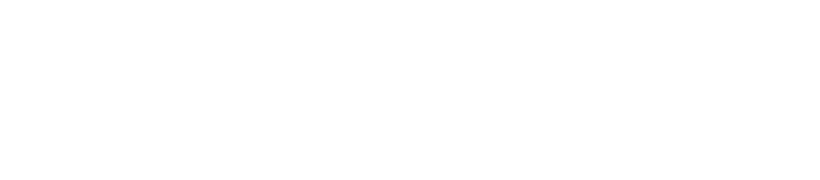
Silicides — alloys of silicon and metals long used in microelectronics — are now being explored again for quantum hardware. But their use faces a critical challenge: achieving phase purity, since some silicide phases are superconducting while others are not.
The study, published in Applied Physics Letters by NYU Tandon School of Engineering and Brookhaven National Laboratory, shows how substrate choice influences phase formation and interfacial stability in superconducting vanadium silicide films, providing design guidelines for improving material quality.
The team, led by NYU Tandon professor Davood Shahrjerdi, focused on vanadium silicide, a material that becomes superconducting (able to conduct electricity without resistance) when cooled below its transition temperature of 10 Kelvin, or about -263°C. Its relatively high superconducting transition temperature makes it attractive for quantum devices that operate above conventional millikelvin temperatures.
Researchers engineered crystalline hafnium oxide substrates and compared them with standard silicon dioxide under identical processing conditions. Hafnium oxide offered greater chemical stability and suppressed unwanted secondary phases, though it degraded under the highest processing temperatures.
"Achieving phase-pure superconducting films requires careful attention to the substrate-film interface," said Shahrjerdi. "Our findings show that substrate design is an integral aspect of the synthesis process.”
The chemical stability of hafnium oxide proved crucial for maintaining film quality during processing. Most intriguingly, atomic-resolution imaging suggested that the crystalline structure of hafnium oxide may influence the orientation and phase selection of overlying silicide grains, pointing to possible templating effects that could enable selective phase nucleation.
The research provides fundamental insights that extend beyond vanadium silicides to other superconducting silicide systems. The principles identified — chemical inertness, thermal stability, and structural ordering — offer design guidelines for next-generation quantum device substrates.
"These findings complement our recent work on physical patterning techniques," noted Shahrjerdi. "Together, they expand the design space for quantum hardware."
In addition to Shahrjerdi, the paper’s authors are Miguel Manzo-Perez, Moeid Jamalzadeh, and Iliya Shiravand (Ph.D. students at NYU Tandon); and Sooyeon Hwang, Kim Kisslinger, and Dmytro Nykypanchuk from the Center for Functional Nanomaterials at Brookhaven National Laboratory. The work was conducted in part at the NYU Nanofabrication Cleanroom (NYU Nanofab) with characterization support from Brookhaven National Laboratory.
Miguel Manzo-Perez, Moeid Jamalzadeh, Sooyeon Hwang, Iliya Shiravand, Kim Kisslinger, Dmytro Nykypanchuk, Davood Shahrjerdi; Substrate effects on phase formation and interfacial stability in superconducting vanadium silicide thin films. Appl. Phys. Lett. 22 September 2025; 127 (12): 122601. https://doi.org/10.1063/5.0291576
NYU Tandon-led team develops new fabrication technique that opens door to new materials for quantum technologies
Researchers have demonstrated a new fabrication approach that enables the exploration of a broader range of superconducting materials for quantum hardware.
The study, published in Applied Physics Letters and selected as a “Featured” article, addresses a long-standing challenge: many promising superconductors, such as transition metal nitrides, carbides, and silicides, are difficult to pattern into functional devices using conventional chemistry-based methods.
By showing that physical patterning provides a viable alternative, the study paves the way to evaluate and harness these materials for high-performing quantum technologies.
The team, led by NYU Tandon professor Davood Shahrjerdi, demonstrated that one such technique, called low-energy ion beam etching (IBE), can be used to fabricate high-performing quantum devices. They validated the approach using niobium, a well-studied superconductor, and benchmarked the resulting devices against state-of-the-art counterparts made with conventional chemistry-based methods, showing comparable performance.
Quantum computers have the potential to tackle problems that are intractable for today's machines, with applications in drug discovery, cryptography, and financial modeling.
"Realizing this promise requires components that can preserve fragile quantum states long enough to perform complex calculations," said Shahrjerdi. "That means building ever more perfect hardware to reduce errors and improve the fault tolerance of quantum systems."
The team's demonstration advances this broader goal by expanding the superconducting material toolkit for device fabrication.
"Fabricating devices with materials-agnostic techniques expands the design space for quantum hardware to under-explored materials, which could catalyze advancements in the scaling of quantum information systems to greater size and functionality," said Dr. Matthew LaHaye, a research physicist at the Air Force Research Laboratory (AFRL) and a collaborator on the project.
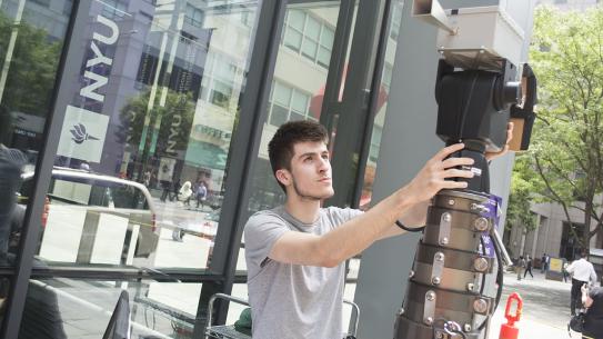
To put this approach to the test, Ph.D. students Miguel Manzo-Perez and Moeid Jamalzadeh, co-lead authors of the study, designed superconducting resonators and developed fabrication protocols that combined electron-beam lithography with IBE. They deposited thin niobium films on silicon substrates and patterned them into superconducting resonators, completing the entire process at the NYU Nanofabrication Cleanroom (NYU Nanofab), the first academic cleanroom in Brooklyn.
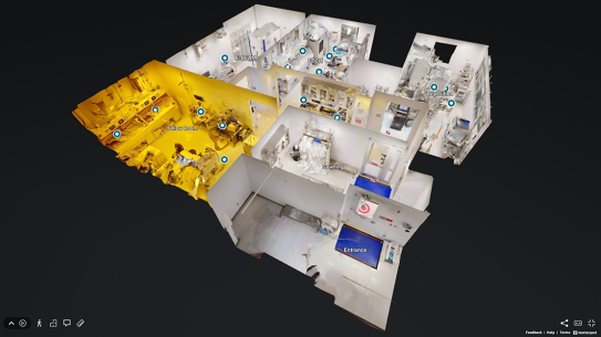
"NYU Nanofab is equipped with state-of-the-art tools and a strategic focus on enabling the fabrication of advanced devices from quantum materials and superconductors," said Shahrjerdi, the inaugural Faculty Director. "In addition to advancing academic research, it also serves as the prototyping facility of the Northeast Regional Defense Technology (NORDTECH) Hub, with the mission to support lab-to-fab transitions in superconducting quantum technologies."
Next, the devices were shipped to AFRL, where Booz Allen Hamilton contractors Christopher Nadeau and Man Nguyen tested them at temperatures near absolute zero. The quantum resonators demonstrated high performance, confirming the feasibility of the IBE-based fabrication approach for realizing low-loss quantum hardware.
Loss is a critical measure of hardware quality, with lower values indicating more perfect superconducting devices.
In addition to Shahrjerdi, LaHaye, Manzo-Perez, Jamalzadeh, Nadeau, and Nguyen, the other co-authors of the paper include Alexander Madden of Booz Allen Hamilton; Iliya Shiravand of NYU Tandon; Kim Kisslinger and Xiao Tong of Brookhaven National Laboratory; Kasra Sardashti of the University of Maryland; and Michael Senatore of the Air Force Research Laboratory.
NYU Tandon and AFRL Rome collaborate under a Cooperative Research and Development Agreement (24-RI-CRADA-09) and are supported by funding from the Microelectronics Commons through the Northeast Defense Technology Hub project entitled "Improved Materials for Superconducting Qubits with Scalable Fabrication."
Miguel Manzo-Perez, Moeid Jamalzadeh, Man Nguyen, Christopher Nadeau, Alexander Madden, Iliya Shiravand, Kim Kisslinger, Xiao Tong, Kasra Sardashti, Michael Senatore, Matthew LaHaye, Davood Shahrjerdi; Physical patterning of high-Q superconducting niobium resonators via ion beam etching. Appl. Phys. Lett. 1 September 2025; 127 (9): 092601. https://doi.org/10.1063/5.0278956

Out of thin air: Researchers create microchips capable of detecting and diagnosing diseases
In a world grappling with a multitude of health threats — ranging from fast-spreading viruses to chronic diseases and drug-resistant bacteria — the need for quick, reliable, and easy-to-use home diagnostic tests has never been greater. Imagine a future where these tests can be done anywhere, by anyone, using a device as small and portable as your smartwatch. To do that, you need microchips capable of detecting miniscule concentrations of viruses or bacteria in the air.
Now, new research from NYU Tandon faculty including Professor of Electrical and Computer Engineering Davood Shahrjerdi; Herman F. Mark Professor in Chemical and Biomolecular Engineering Elisa Riedo; and Giuseppe de Peppo, Industry Associate Professor in Chemical and Biomolecular Engineering and who was previously at Mirimus, shows it’s possible to develop and build microchips that can not only identify multiple diseases from a single cough or air sample, but can also be produced at scale.
“This study opens new horizons in the field of biosensing. Microchips, the backbone of smartphones, computers, and other smart devices, have transformed the way people communicate, entertain, and work. Similarly, today, our technology will allow microchips to revolutionize healthcare, from medical diagnostics, to environmental health” says Riedo,
“The innovative technology demonstrated in this article uses field-effect transistors (FETs) — miniature electronic sensors that directly detect biological markers and convert them into digital signals — offering an alternative to traditional color-based chemical diagnostic tests like home pregnancy tests,” said Shahrjerdi. “This advanced approach enables faster results, testing for multiple diseases simultaneously, and immediate data transmission to healthcare providers” says Sharjerdi, who is also the Director of the NYU Nanofabrication Cleanroom, a state-of-the-art facility where some of the chips used in this study were fabricated. Riedo and Shahrjerdi are also the co-directors of the NYU NanoBioX initiative.
Field-effect transistors, a staple of modern electronics, are emerging as powerful tools in this quest for diagnostic instruments. These tiny devices can be adapted to function as biosensors, detecting specific pathogens or biomarkers in real time, without the need for chemical labels or lengthy lab procedures. By converting biological interactions into measurable electrical signals, FET-based biosensors offer a rapid and versatile platform for diagnostics.
Recent advancements have pushed the detection capabilities of FET biosensors to incredibly small levels — down to femtomolar concentrations, or one quadrillionth of a mole — by incorporating nanoscale materials such as nanowires, indium oxide, and graphene. Yet, despite their potential, FET-based sensors still face a significant challenge: they struggle to detect multiple pathogens or biomarkers simultaneously on the same chip. Current methods for customizing these sensors, such as drop-casting bioreceptors like antibodies onto the FET’s surface, lack the precision and scalability required for more complex diagnostic tasks.
To address this, these researchers are exploring new ways to modify FET surfaces, allowing each transistor on a chip to be tailored to detect a different biomarker. This would enable parallel detection of multiple pathogens.
Enter thermal scanning probe lithography (tSPL), a breakthrough technology that may hold the key to overcoming these barriers. This technique allows for the precise chemical patterning of a polymer-coated chip, enabling the functionalization of individual FETs with different bioreceptors, such as antibodies or aptamers, at resolutions as fine as 20 nanometers. This is on par with the tiny size of transistors in today’s advanced semiconductor chips. By allowing for highly selective modification of each transistor, this method opens the door to the development of FET-based sensors that can detect a wide variety of pathogens on a single chip, with unparalleled sensitivity.
Riedo, who was instrumental in the development and proliferation of tSPL technology, sees its use here to be further evidence of the groundbreaking way this nanofabrication technique can be used in practical applications. “tSPL, now a commercially available lithographic technology, has been key to functionalize each FET with different bio-receptors in order to achieve multiplexing,” she says.
In tests, FET sensors functionalized using tSPL have shown remarkable performance, detecting as few as 3 attomolar (aM) concentrations of SARS-CoV-2 spike proteins and as little as 10 live virus particles per milliliter, while effectively distinguishing between different types of viruses, including influenza A. The ability to reliably detect such minute quantities of pathogens with high specificity is a critical step toward creating portable diagnostic devices that could one day be used in a variety of settings, from hospitals to homes.
The study, now published by the Royal Society of Chemistry in Nanoscale, was supported by Mirimus, a Brooklyn-based biotechnology company, and LendLease, a multinational construction and real estate company based in Australia. They are working with the NYU Tandon team to develop illness-detecting wearables and home devices, respectively.
“This research shows off the power of the collaboration between industry and academia, and how it can change the face of modern medicine,” says Prem Premsrirut, President and CEO of Mirimus. “NYU Tandon’s researchers are producing work that will play a large role in the future of disease detection.”
“Companies such as Lendlease and other developers involved in urban regeneration are searching for innovative solutions like this to sense biological threats in buildings.” says Alberto Sangiovanni Vincentelli of UC Berkeley, a collaborator on the Project. “Biodefense measures like this will be a new infrastructural layer for the buildings of the future”
As semiconductor manufacturing continues to advance, integrating billions of nanoscale FETs onto microchips, the potential for using these chips in biosensing applications is becoming increasingly feasible. A universal, scalable method for functionalizing FET surfaces at nanoscale precision would enable the creation of sophisticated diagnostic tools, capable of detecting multiple diseases in real time, with the kind of speed and accuracy that could transform modern medicine.
Research Centers, Labs, and Groups

NYU WIRELESS
NYU WIRELESS is an innovative academic research center with a focus on 6G and beyond, and from mmWave to Terahertz

Center for Advanced Technology in Telecommunications (CATT)
Creating economic impact through research, technology transfer, and faculty entrepreneurship.