Nano-Scale Electronics Score Laboratory Victory
NYU Tandon Researchers Pioneer Technique to Grow Monolayer Tungsten Disulfide for Next-Generation Transistors, Wearable Electronics, and Biomedical Devices

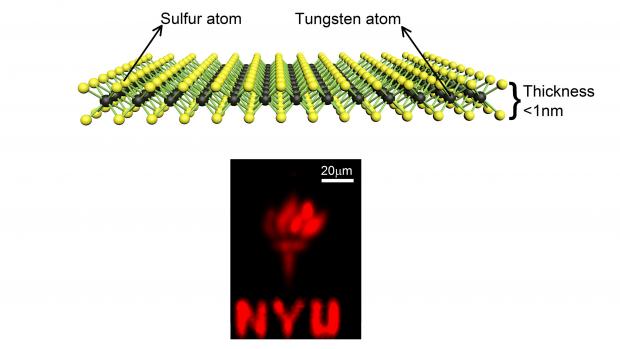
At just one atom thick, tungsten disulfide allows energy to switch off and on, but it also absorbs and emits light, which could find applications in optoelectronics, sensing, and flexible electronics. The NYU logo shows the monolayer material emitting light.
Researchers at the NYU Tandon School of Engineering have pioneered a method for growing an atomic scale electronic material at the highest quality ever reported. In a paper published in Applied Physics Letters, Assistant Professor of Electrical and Computer Engineering Davood Shahrjerdi and doctoral student Abdullah Alharbi detail a technique for synthesizing large sheets of high-performing monolayer tungsten disulfide, a synthetic material with a wide range of electronic and optoelectronic applications.
“We developed a custom reactor for growing this material using a routine technique called chemical vapor deposition. We made some subtle and yet critical changes to improve the design of the reactor and the growth process itself, and we were thrilled to discover that we could produce the highest quality monolayer tungsten disulfide reported in the literature,” said Shahrjerdi. “It’s a critical step toward enabling the kind of research necessary for developing next-generation transistors, wearable electronics, and even flexible biomedical devices.”
The promise of two-dimensional electronic materials has tantalized researchers for more than a decade, since the first such material — graphene — was experimentally discovered. Also called “monolayer” materials, graphene and similar two-dimensional materials are a mere one atom in thickness, several hundred thousand times thinner than a sheet of paper. These materials boast major advantages over silicon — namely unmatched flexibility, strength, and conductivity — but developing practical applications for their use has been challenging.
Graphene (a single layer of carbon) has been explored for electronic switches (transistors), but its lack of an energy band gap poses difficulties for semiconductor applications. “You can’t turn off the graphene transistors,” explained Shahrjerdi. Unlike graphene, tungsten disulfide has a sizeable energy band gap. It also displays exciting new properties: When the number of atomic layers increases, the band gap becomes tunable, and at monolayer thickness it can strongly absorb and emit light, making it ideal for applications in optoelectronics, sensing, and flexible electronics.
Efforts to develop applications for monolayer materials are often plagued by imperfections in the material itself — impurities and structural disorders that can compromise the movement of charge carriers in the semiconductor (carrier mobility). Shahrjerdi and his student succeeded in reducing the structural disorders by omitting the growth promoters and using nitrogen as a carrier gas rather than a more common choice, argon.
Shahrjerdi noted that comprehensive testing of their material revealed the highest values recorded thus far for carrier mobility in monolayer tungsten disulfide. “It’s a very exciting development for those of us doing research in this field,” he said.
The researchers received support from the National Science Foundation and the Center for Functional Nanomaterials at Brookhaven National Laboratory. The paper, Electronic Properties of Monolayer Tungsten Disulfide Grown by Chemical Vapor Deposition, is available at scitation.aip.org/content/aip/journal/apl/109/19/10.1063/1.4967188.
About the NYU Tandon School of Engineering
The NYU Tandon School of Engineering dates to 1854, when the New York University School of Civil Engineering and Architecture as well as the Brooklyn Collegiate and Polytechnic Institute (widely known as Brooklyn Poly) were founded. Their successor institutions merged in January 2014 to create a comprehensive school of education and research in engineering and applied sciences, rooted in a tradition of invention, and entrepreneurship and dedicated to furthering technology in service to society. In addition to its main location in Brooklyn, NYU Tandon collaborates with other schools within the country’s largest private research university and is closely connected to engineering programs in NYU Abu Dhabi and NYU Shanghai. It operates business incubators in downtown Manhattan and Brooklyn and an award-winning online graduate program.


